ISSCC 2024 Circuit Insights
Written by Morris Fan @Marriott Hotel, San Francisco, Feb. 17, 2024
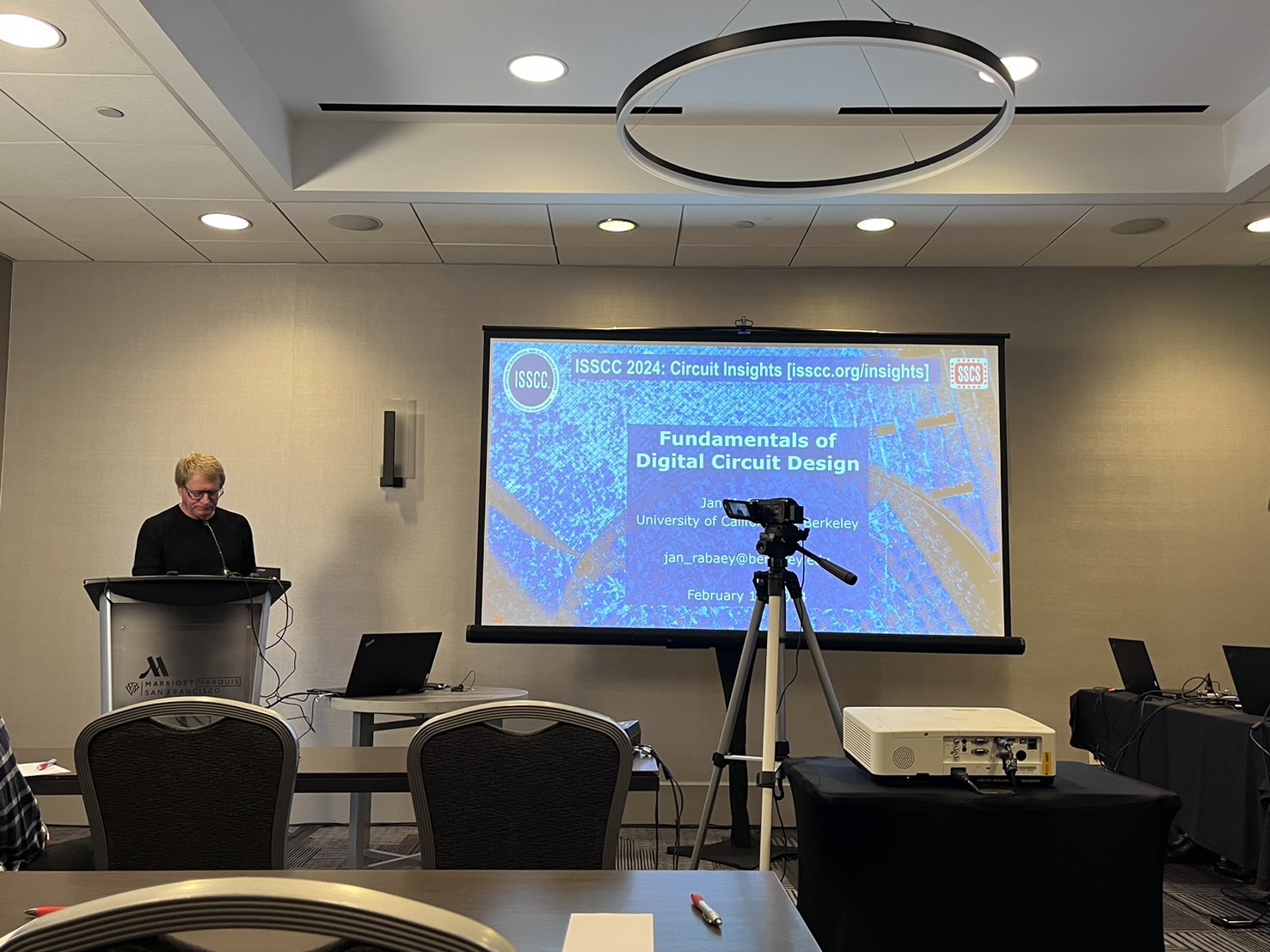
Fundamentals of Digital Circuit Design
Prof. Jan M. Rabaey, University of California, Berkeley USA
Compute, Communicate, Acquire/Act
In digital design and computing, we focused on complexity at low cost.
From the lower level to the top: Boolean (0 and 1), logic gate control, processor, and memories to software.
We use VOLTAGE representation for signals (current, flux can also but no). Voltage signals are not ideal since it is affected by the environment, couple, and noises. We define threshold range.
Regeneration: no accumulation of noise in complex circuits.
- In contrast to analog circuits. Which allows you to stack up circuits.
In the digital world, we view transistors as switches. However, it is not ideal and determines speed (performance) and energy consumption, caused by parasitic caps and resistance (Cs, Cd, Ron, Roff).
Charge and discharge caps, delay
Energy and power:
-
Switching (dynamic consumption) =
-
Static consumption =
Modularity and hierarchy:
- Combine Easy composability to get a modular design approach.
- Delay = D1+D2
- Hierarchy to handling complexity
- F = (F1, F2) functions
Timing and Sequential Circuits:
-
Asynchronous design is not ideal
-
The absolute, time reference, clock synchronizes Clk to ensure function completion and order execution steps to achieve that once the signal passes clk, the signal is stable. Clk can’t be too fast, o.w. Clk edges are subject to delay (skew) and noise (jitter)
-
Provide timing margins to offset worst-case scenarios
-
Optimize clk distribution network
Verification:
- Functionality
- Signal noise margins
- Timing margins
- Optimize and repetition
Jitter impact: 2 wires too close to each other (coupling caps btw the wires), bad clk, minimize the variance, solve by adding buffers.
Q: Asynchronous clk is not useful since it didn’t have great EDA, is it worth developed?
R: Only triggered when the signal is changing, so the time variance is large, and we are doing worst case circuits, so it’s hard to design timing margin.
- SPICE doesn’t scale in billions of transistors.
Design methodology:
- Verification and design automation (freedom from component choice)
- To make a reliable circuit, Always Stick to the design rules.
Design productivity: transistor-level => gate level => register transfer level (RTL) => reuse => AI design tools? => AI designing computers? (What’s the rule and the role of the designer?)
Verilog:
- Structure: HOW
- Behavior: WHAT
Reuse the block
Raising the bar, start using Python, java, tensor flow => the generator (ex. RISC-V)
As we are approaching the physical limitation. The ingenuity of humans and the ingenuity of nature, are there any natural models (different aspects)?
Q: Why don’t we redesign the gate levels to increase the performance? Since you also need to redesign the verifications. choose the now that WINS. Will AI do the verification faster?
R: Cost time and efforts.
Q: Any other physical materials other than silicon to push regeneration. Quantum? Neural?
R: Sometimes you are not able to consider worst case scenario, like Gaussian distribution? Put circuits for detection, error correction to assist design.
Q: Ideas on Moore’s law?
R: Increase density, CFet (PMOS over NMOS).
CMOS Circuit for Biomedical Applications
Prof. Carolina Mora Lopez, IMEC, Leuven, Belgium
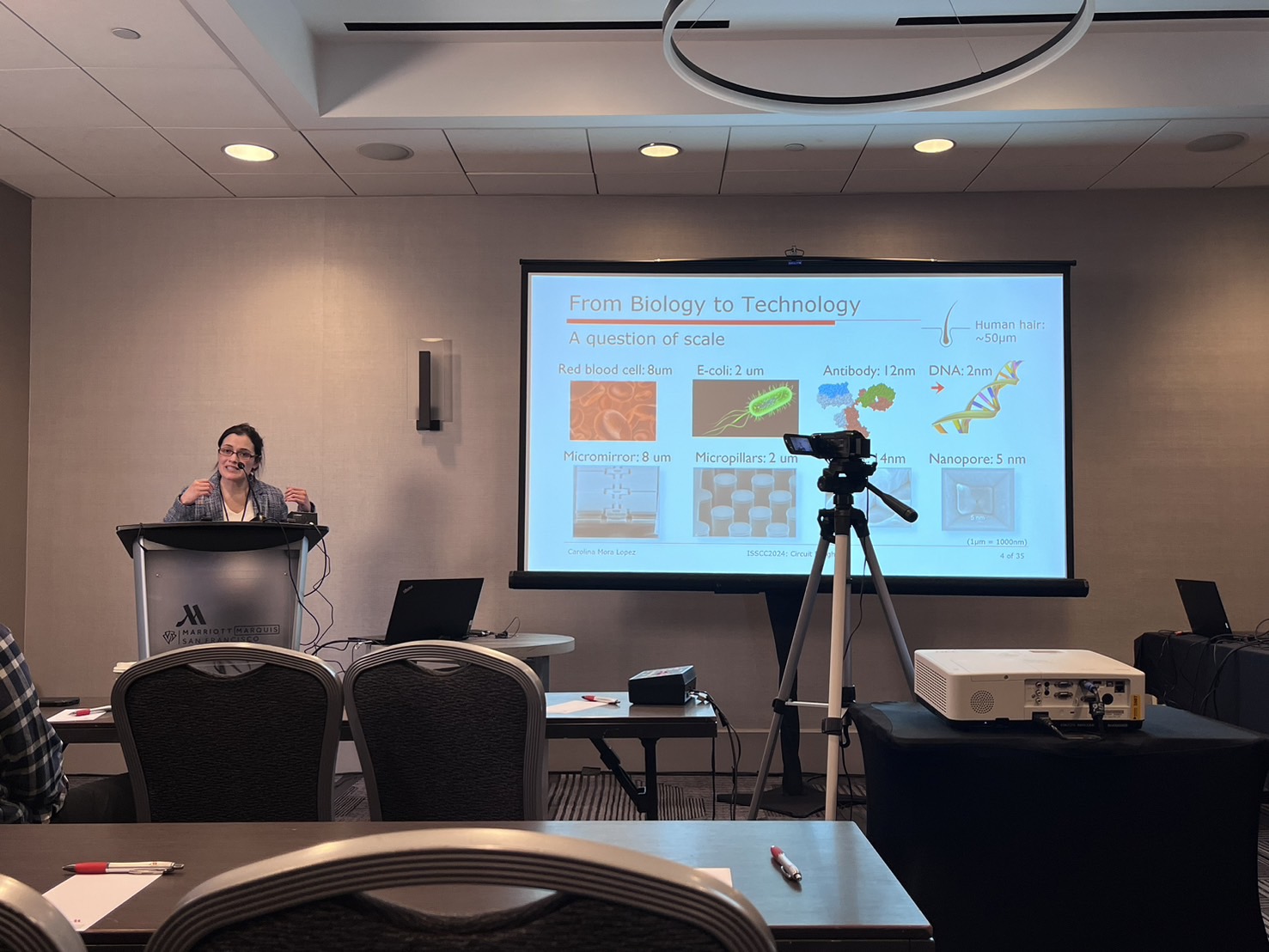
The complexity of the human brain v.s. technology.
Aiming to manage disease, ease pain……
How can we interface with technology?
- Sense: getting information from bio-electric signals
- Actuate: Drive a certain organ
Problem 1: Electrical noise
-
Thermal noise
- a.k.a. white noise (noise for static resistance generated by the random thermal motion of charge carriers)
-
Flicker noise
- a.k.a. white noise (1/f noise) in transistors is caused by imperfections in the crystalline structure of semiconductors
-
Noise spectrum
- avg noise power at each frequency
-
Corner frequency
- where two noises coincide
- Biopotential signals are low-frequency signals
- Must minimize Both noises
-
Design Trade-offs
- area v.s. noise and power v.s. noise
Interface with Biology
-
Cell, electro-chemical reactions
-
Electrode is the electrical interface between tissue and electronics.
Problem 2: Electrode DC Offset (EDO)
-
How do you design your amplifier?
-
Half-cell potential might be positive or negative depending on the material
-
Electrode impedance magnitude decreases as the frequency gets higher
-
-
Achieving a high impedance in AC
-
Small = low Zin @DC, for AC, is not that straightforward
-
Vin = vbio + VEDO, EDO should not be an amplifier.
-
-
How to remove EDO?
-
High pass filter, reject fc < 1Hz
-
Make zin > 10*Zele to reduce noise.
-
Biopotential Amplifier General Metrics (Spec of bio-amp)
- Low noise
- Can reject EDO
- High input impedance
- Application spec requirement:
- Small area
- Low power
- Good linearity
- Low input leakage (BJT has input current which is deserted)
Complete biopotential readout
- Recording electrode
- low-noise amp (the one that wants to be optimized) +
- filter
- programmable gain amplifier
- ADC (determine signal quality, how many bits/levels required)(but not over-designed, expensive, enough is enough, more bits
- more power needs to compute)
LNA
- Negative Feedback loop diff amp
- Pseudo-resistors
-Diode-connected MOS biased in cut-off
-The equivalent resistance values > 100G ohms
-Small area
-non-linear
-temperature dependent
- Pseudo-resistors
Differential amplifier
Upper PMOS (Mpi) dominates the noise
To achieve low noise
- large gm in Mpi for PMOS input pairs
- small gm in Mnb for NMOS active loads (lower MOS in the right bottom)
Multi-channel readout
Multi-channel readout can enable high-density sensing
Neural readout ASIC
-
Neuro-probe
- Brain behaviors (SoC)
- Time-division multiplexing
-
Needles
Summary
Biopotential are small (uV-mV) and low-frequency (<10kHz) signals
Q: Neural link claimed they have implanted a ‘brain-reading’ device into a person. allowing a person with severe paralysis to control a computer, robotic arm, wheelchair or other device through thought alone. What do you think of the future of putting chips to normal human beings or it should stick with medical usage.
R: Yes, it might happened, this is not the first approach people claims to put chips into human brains. it is high risks procedures, some day it might be in customer electric such as gaming and daily lives.
Q: Battery and power
R: Power supplies, when to charge the device and how often should you charge the device. Noise cancellation to decrease power consumption
Lunch Networking

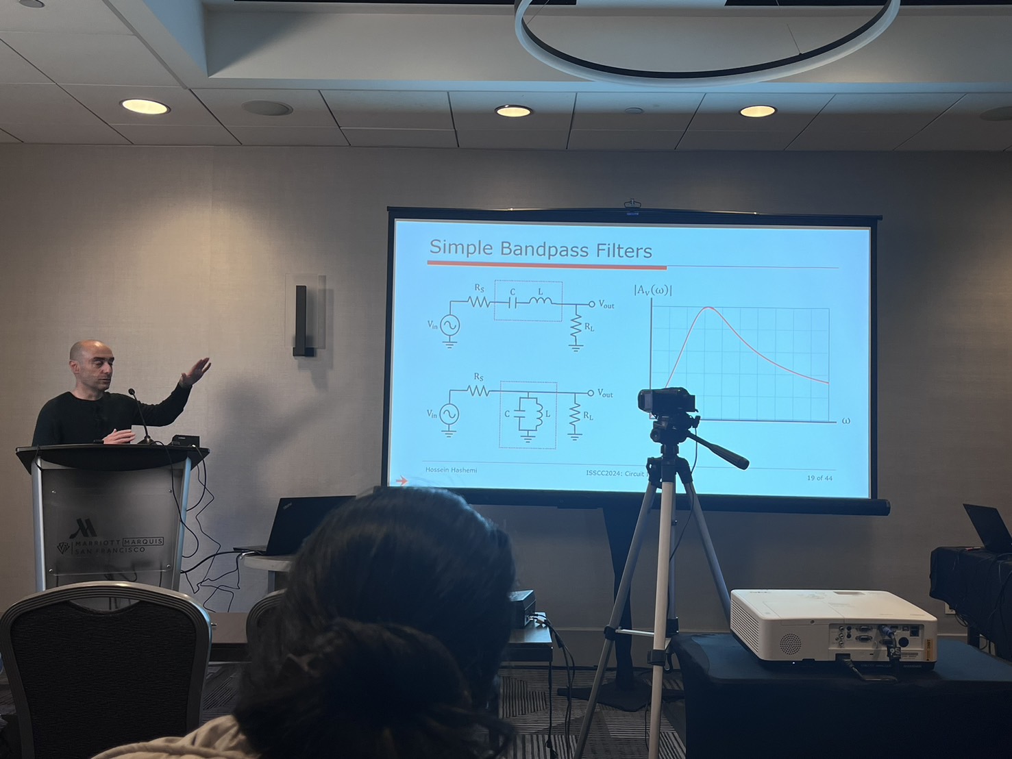
The Basic of Ratio Frequency (RF) Circuits
Prof. Hossein Hashemi, University of Southern California, USA
In the air, EM waves travel at the speed of light.
-
Propagation speed is lower in another
-
The electric and magnetic fields vary with time as sinusoids.
-
The propagating wave is periodic in space as well.
-
Wavelength is the special of the EM wave.
-
-
RF refers to wavelength btw , if the wavelength is long enough, it is available to see behind the wall.
Modulation is the process of extracting the information signal from a modulated carrier signal.
Radiofrequency transmitter modulator
Radio frequency receiver demodulator
-
Modern radio frequency receiver
- Signal => bandpass filter => ......
-
Average power consumption of resistors =
-
For caps (current is the derivative of voltage): sometimes it gives power, sometimes stores power.
-
Parasitic caps create a low-impedance path at high frequency. (Vout becomes zero at high frequency).
- In order to create a bandpass filter, we want to resonate, so we add an inductor parallel to the caps.
The hardest part is power amplifier to transmit the signal over a longer distance.
The problem is that if the device consumes large power, it requires high voltage too. But circuits now consume voltage less than 1V. and the antenna resistance is fixed.
Instead, we use transformers (2 inductors)
Impedance transformer: CM connected to (LM to gnd). Comments “emoter”
Oscillator:
- During LC resonate, no energy is lost.
- T = 2pi(LC)^0.5
RF Mixers:
-
An LTI system cannot multiply two signals.
- Switching mixer (Vcontrol > 0 = on)
-
Any periodic waveform can be represented using Fourier series
By Fourier series, we get the desired signal but also a bunch of unwanted signals, but we got a bandpass filter.
Summary:
- Modern RF circuits use analog and digital techniques.
- Important concepts related to RF circuits: noise, linearity……
- RFIC designers are in high demand
Q: When the frequency is low enough, we can easily generate sine and cosine. But for higher frequency it is not energy efficient.
R: Information separated to I and Q, multiply with oscillator(carrier wc) in between and add(using KCL) them together.
Q: Driving force between RF industry? pushing frequency higher to get different part of wavelength. Inductors and caps for resonate are large, occupied lots of area. Can we replace inductor?
R: Tunnel creation: focus the beam like a laser, spacial diversity
- Technics to reduce parasitic caps, literally minimize length and width of wires, make circuit compact or 4 RF circuit, resonate cancelled out. make Transmission line
Q: Negative caps?
R: Noise linearity issue
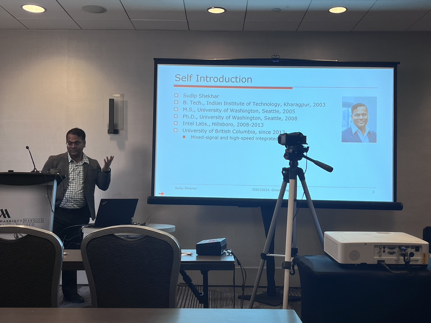
The Basic of Silicon-Photonic Circuits
Prof. Sudip Shehkar, University of British Columbia, Canada
Improve performance:
- speed
- latency
- parallelism //CMOS
Transceiver:
- transmitter and receiver
Miniaturize discrete or bulky components //RF-CMOS
CMOS SOI (Silicon on Insulator)
Enable new application:
- Silicon photonics CMOS SOI
CMOS strengths and weaknesses
Great:
- High gain
- switching
- generating clock frequency up to 100s of GHz
Realizing complex functions with billions of transistors on a single chip
Limitation:
- Having limitations driving high-speed data from one chip to another over a long distance, due to Cu loss, interacting(sensing, detecting) with different particles and waves.
Silicon photonics:
- new tech
- promising to Complement some challenges ex. Increase speed, reduce latency, and reduce power.
- Usage in data center, cloud
- Shrink the LIDAR on a small chip to lower the cost.
- Data centers are connected to optical fiber.
Frequency-dependent loss in the Cu channel creates inter-system interferences (ISI)
Loss increases at high rates and loss increases with the length of interconnect => Equalizer helps. But consumes power
Get rid of fiber, instead, using optical fiber for cable (less attenuated), and change the source to laser (tera Hz), couple the laser into photonic chip => silicon photonic
Optical switch (modulator) to block the laser-driven by electronic. (amplitude modulation)
Fiber sending:
- different lengths
- different light
- less interrupt with each other
- Support multiple data streams, each on a separate wavelength, on the same waveguide of fiver (WDM)
Electro-optical link:
- since now we are talking about terahertz, the wavelength is extremely small, so we need electronic control.
Y-branch splitter:
- 50/50 intensity splitter with output ports identical in phase
Photodetector/photodiodes (PDs)
- Produce current from current phonons
Passives:
- Mach-Zehnder interferometer (MZI) //split then add up
- , so we control the modulator by different phase shifts.
- By adding different voltages, we get different phase shifts, and we get the current
N is a measure of the reduction of the velocity of light in a medium vs vacuum, .
Change n to change velocity,
Thermal phase shifter (TPS):
- add a metal resistor near the Si waveguide, heating up when a current flows through it.
High-speed phase shifter:
- Dope the Si rib waveguide to make a p-n junction
The diode also has parasitics caps, so we use transmission lines to lower caps or cancel out with inductors.
Put both electronics and photons in Si-process: cointegrated and ……
Biosensors:
- sensing refractive index, ring resonator (bandpass filter).
- We can drop blood on this ring to detect COVID-19 viruses, and we can scale it into other COVID-19 alpha, beta……
Q: Send info with time as reference
R: Synchronize
Pulse amplitude modulation
Noise consideration about the PN junction modulator?
Q: Do I need to worry about refraction?
R: Not a problem for the high-speed circuit. What's the case we want refraction? Surface grating coupling, use it to combine lights.
Copyright © 2024, Chih-Chieh (Morris) Fan
All rights reserved. Please mention my name and source code for reference.